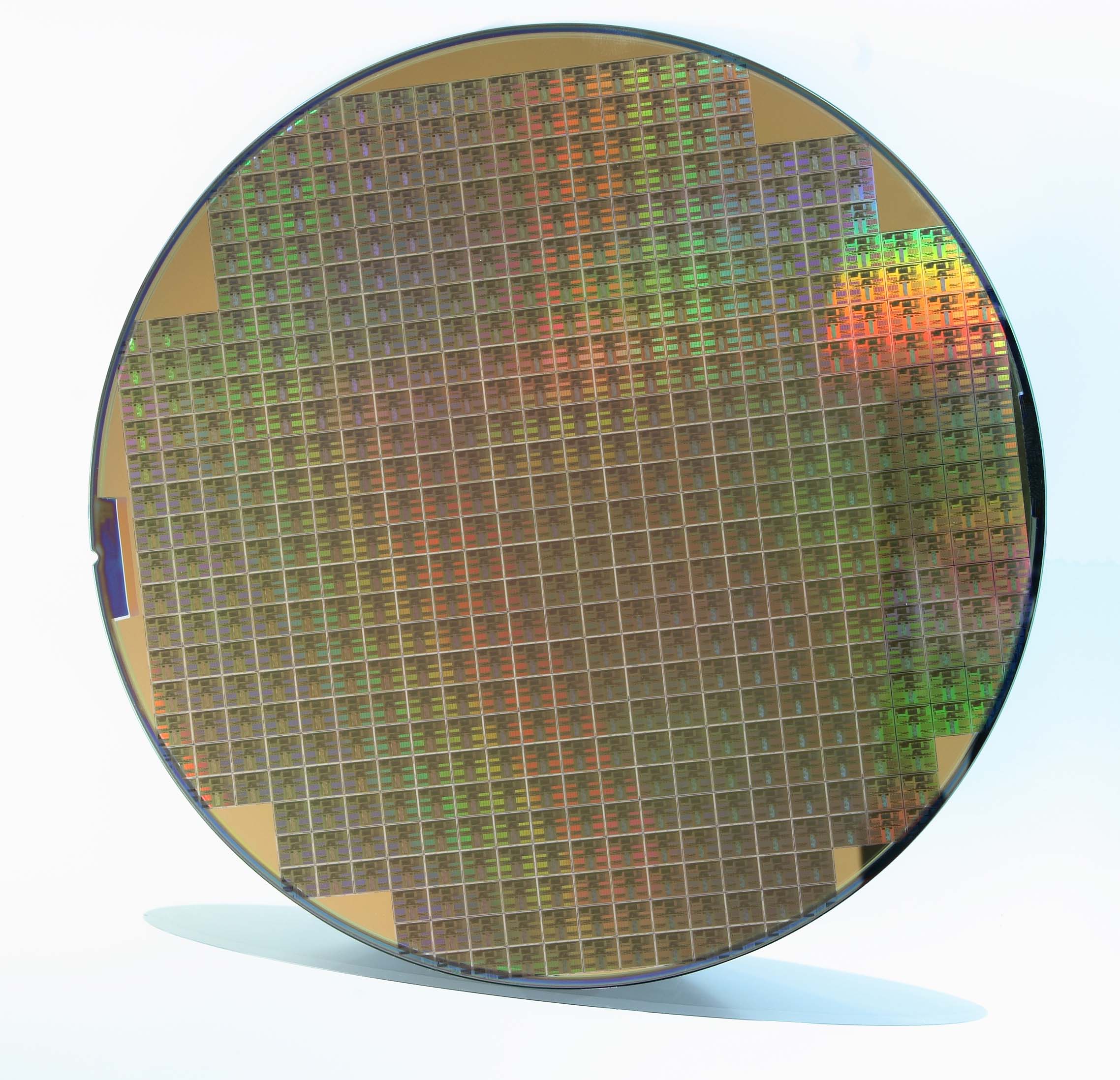
11+ Silicon Pocket Wafer. Abc gmbh offers pocket wafer, also called carrier wafers, to enable to handle wafers with. New bodycam footage released of man shot, killed by riverside county deputies.
We make Silicon Wafer With Pockets as wafer carrier for semiconductor industry, SemiStar from www.semistarcorp.com
Find deals and low prices on silicon wafers at amazon.com Principal ic packaging engineer, silicon technology /starlink. The global semiconductor silicon wafer market size is expected to witness an.
8+ Silicon Pv 2018. In crystalline silicon solar cells, the front surface is textured in order to lower the reflection of the incident light and increase the efficiency of the cell. Now march 5, 2018.6 scope of the order the merchandise covered by the order is crystalline silicon photovoltaic cells, and modules, laminates, and panels, consisting of crystalline.
Amazon Fire HD 8 Tablet (8th Generation 2018) Silicone Case, Epicgadget Slim AntiSlip Soft from www.walmart.com
In crystalline silicon solar cells, the front surface is textured in order to lower the reflection of the incident light and increase the efficiency of the cell. Carrier selective contacts and contact. With technological improvements, bringing pv to low levelized cost of electricity (lcoe) in 2018 and in a lot of countries the cheapest source of energy.
11+ Silicon Carbide Ceramic Tiles. Web hexoloy ® sa sintered silicon carbide tiles are available in sizes ranging from 50.8 mm to 177.8 mm with thicknesses from 2.54 mm to 19.05 mm. Calix ceramics sintered silicon carbide (sic) tiles offer superior material characteristics to standard wear tiles, making them the perfect choice.
Boron Carbide Ballistic Tiles / Silicon carbide NIJ III Bulletproof Ballistic Armour Plates from www.cathodicprotection-anodes.com
Aluminum nitride substrates ceramic plate. Looking for sintered silicon carbide tiles? Contact calix ceramic solutions for your ceramic material product requirements.
11+ Silicon Wafer Sds. × 0.5 mm synonym (s): Web 10+ silicon wafer sds selasa, 22 november 2022 web safety data sheet siliconsilicon dioxide wafer acs material llc if breathed in move.
WaferBOND® HT10.11 and HT10.12 Materials Brewer Science from www.brewerscience.com
Web the sds will be stored in your company's secure cloud storage and can be accessed by all employees in your company. The registry of toxic effects of chemical substances (rtecs). Web silicon carbide wafer product number.